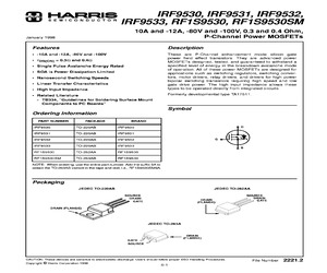
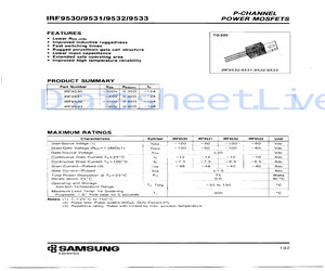
IRF9532, IRF9533, RF1S9530, RF1S9530SM 10A and -12A, -80V and -100V, 0.3 and 0.4 Ohm, P-Channel Power MOSFETs January 1998 Features Description * -10A and -12A, -80V and -100V These are P-Channel enhancement mode silicon gate power field effect transistors. They are advanced power MOSFETs designed, tested, and guaranteed to withstand a specified level of energy in the breakdown avalanche mode of operation. All of these power MOSFETs are designed for applications such as switching regulators, switching convertors, motor drivers, relay drivers, and drivers for high power bipolar switching transistors requiring high speed and low gate drive power. The high input impedance allows these types to be operated directly from integrated circuits. * rDS(ON) = 0.3 and 0.4 * Single Pulse Avalanche Energy Rated * SOA is Power Dissipation Limited * Nanosecond Switching Speeds * Linear Transfer Characteristics * High Input Impedance Formerly developmental type TA17511. * Related Literature - TB334, "Guidelines f
 7 Pages, 54 KB, Original
IRF9532, semrconpuceto IR F9533, RF1S9530, RF1S9530SM 10A and -12A, -80V and -100V, 0.3 and 0.4 Ohm, January 1998 P-Channel Power MOSFETs Features Description -10A and -12A, -80V and -100V These are P-Channel enhancement mode silicon gate . _ power field effect transistors. They are advanced power "DS(ON) = 9.32 and 0.40 MOSFETs designed, tested, and guaranteed to withstand a + Single Pulse Avalanche Energy Rated specified level of energy in the breakdown avalanche mode . ooo. i. of operation. All of these power MOSFETs are designed for * SOA is Power Dissipation Limited applications such as switching regulators, switching conver- + Nanosecond Switching Speeds tors, motor drivers, relay drivers, and drivers for high power . , bipolar switching transistors requiring high speed and low + Linear Transfer Characteristics gate drive power. The high input impedance allows these + High Input Impedance types to be operated directly from integrated circuits. * Related Literature Formerly developmental typ
 7 Pages, 161 KB, Scan
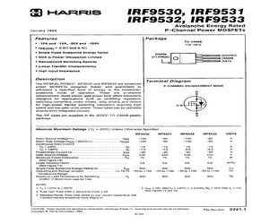
er MOSFETs -10A, and -12A, -60V and -100V pston = 0.300 and 0.400 Features: Single pulse avalanche energy rated = SOA is power-dissipation limited s Nanosecond switching speeds a Linear transfer characteristics = High input impedance The IRF9530, IRF9531, IRF9532 and IRF9533 are advanced power MOSFETs designed, tested, and guaranteed to withstand a specified level of energy in the breakdown avalanche mode of operation. These are p-channel en- hancement-mode silicon-gate power field-effect transistors designed for applications such as. switching regulators, switching converters, motor drivers, relay drivers, and drivers for high-power bipolar switching transistors re- quiring high speed and low gate-drive power. These types IRF9530, IRF9531 IRF9532, IRF9533 TERMINAL DIAGRAM o 92CS-43262 P-CHANNEL ENHANCEMENT MODE TERMINAL DESIGNATION DRAIN ~ (FLANGE) CO can be operated directly from integrated circuits Tor view GATE The IRF-types are supplied in the JEDEC TO-220AB plastic 9208-39528 p
 5 Pages, 195 KB, Scan
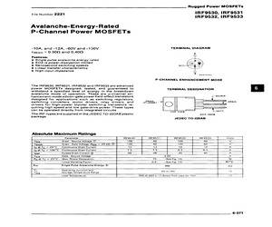
IRF9532, IRF9533 January 1994 Avalanche Energy Rated P-Channel Power MOSFETs Features -10A and -12A, -80V and -100V * FDS(ON) = 0.32 and 0.42 Single Pulse Avalanche Energy Rated * SOA is Power-Dissipation Limited Nanosecond Switching Speeds * Linear Transfer Characteristics * High Input Impedance Description The IRF9530, IRF9531, IRF9532 and IRF9533 are advanced power MOSFETs designed, tested, and guaranteed to withstand a specified level of energy in the breakdown Package TO-220AB TOP VIEW DRAIN > SOURCE (FLANGE) O | ===> DRAIN | | _ > cate Terminal Diagram P-CHANNEL ENHANCEMENT MODE (0.063 (1.6mm) from case for 10s) NOTES: 1. Ty = +25C to +150C 2. Pulse Test: Pulse width < 300ys,Duty Cycle < 2% 3. Repetitive Rating: Pulse width limited by max. junction temperature. See Transient Thermal impedance Gurve (Figure 5) avalanche mode of operation. These are p-channel D enhancement-mode silicon-gate power field-effect transistors designed for applications such as switching regulators, swi
 5 Pages, 182 KB, Scan
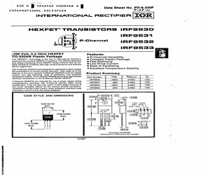
S DS(on) Ip | . IRF9530 -100V 0.309 -12A P-Channel HEXFETs are intended for use in power stages where complementary symmetry with N-Channel devices offers circuit IRF9531 ~60V 0.302 -12A simplification. Thay are also very useful in drive stages because of IRF9532 -100V 0.402 -10A the circuit versatility offered by the reverse polarity connection. Applications include motor control, audio amplifiers, switched mode IRF9533 -60V 0.402 -10A converters, control circuit and pulse amplifiers. 4041 TERM 4 CASE STYLE AND DIMENSIONS servant Hr oeemetsho| TERM T6210 103) | 3 79 (0.1495 L- 132 (0.052) 4 | 0 1397 122(0 048) = 648 (0 255) 10.54 (0.415) . | 625 (02451 TERM 3 - SOURCE TERM Z -ORAIN MAX. 1509 (0 5941 14 84 (05841 TERM 1 - GATE WW 45) Mi TT 5 (0.45) MIN 1570 a0) _ $320 170) 1 15.09 (0.694) tr rau] MAX 396 (0 156) 229 (0090) - . 385 (0 140) 533 (0.2t0) 13.97 (0550) Sag sar 1347 (0530) x) f* J SECTION X-X 51 (0.020) 47018) Cc] ao F | | 0939 (0.037) 140 (2 088) a 0 686 (0.0271 115 {0 045} 289 (0 144)
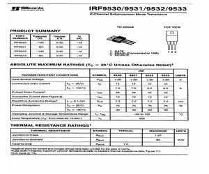
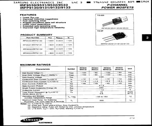
 6 Pages, 449 KB, Scan
Fast switching times Rugged polysilicon gate cell structure Lower input capacitance Extended safe operating area Improved high temperature reliability PRODUCT SUMMARY Part Number Vos Roston) i) IRF9530 ~100v | 0.309 | -12A IRF9531 -eov | 0.309 | -12A |____IRF9532 -100v! 0.400 -10A, IRF9533 . 60v| 0.409 | -10A MAXIMUM RATINGS TO-220 IRF 9530/953 1/9532/9533 | IRF9532 Characteristic Symbol IRF9530 IRF9531 IRF9533 Unit | Drain-Source Voitage {1} oo Voss _ | -100 _{.. 760 | 100 60 Vde __Drain-Gate Voltage (Res=1.0MM)(1) _Nocr 100 L 760 | =100 | -60 Vde __Gate-Source Voltage - Ves ae +20 cpt Vde __Continuous Drain Current To=25 c lp L.o7 12 -12. | -10 [ 71 o | Ade | | Continuous Drain Current Te = 100C Ip | 778 75 | 65 765 Adc Drain CurrentPulsed (3) IDM : 48 | 48 | 40 | 40 Adc _ Gate CurrentPulsed _ lom #15 Adc Total Power Dissipation @ Tc=25C Pp 75 Watts | Derate above 25C | oo _ 0.6 - (C | Caan Temporaere Range | TH T80 79810190. c | Purposes. 1/8" from case for S seconds, + _| 300 *c
 5 Pages, 182 KB, Scan
IRF9532 -100 0.40 -10 IRF9533 -60 0.40 -10 IRF9530/9531/9532/9533 P-Channel Enhancement Mode Transistors TO-220AB TOP VIEW Oo 1 GATE 123 2 DRAIN (Connected to TAB) 3 SOURCE ABSOLUTE MAXIMUM RATINGS (Tc = 25C Unless Otherwise Noted)! IRF PARAMETERS/TEST CONDITIONS SYMBOL 9530 9531 9532 9533 | UNITS Gate-Source Voltage Ves +20 +20 +20 +20 Vv Continuous Drain Current Te = 25C Ip 12 12 10 10 To = 100C 7.5 7.5 6.5 6.5 A Pulsed Drain Current? lom 48 48 40 40 Avalanche Current (See Figure 9) laR 12 12 12 12 Repetitive Avalanche Energy? L = 0.1 mH Ear 7.2 7.2 7.2 7.2 mJ Power Dissipation To = 25C Pp 75 75 75 75 Ww To = 100C 30 30 30 30 Operating Junction & Storage Temperature Range | Ty, Tstg -55 to 150 C Lead Temperature ('/,, from case for 10 sec.) Tr 300 THERMAL RESISTANCE RATINGS" THERMAL RESISTANCE SYMBOL TYPICAL MAXIMUM UNITS Junction-to-Case Rinsc 1.67 Junction-to-Ambilent Rina 80 K/W Case-to-Sink Rincs 1.0 ty Negative signs for current and voltage ratings have been omitted for the sake of clarity
 4 Pages, 237 KB, Scan
3 SIEG IRF132 3 GESY RFP6P08 2 RCA VNO350N5 2 STX SIEG TX4N50P 1 TXC MTP8N45 3 MOTA IRF9512 3 INR VP1204N5 2 STX 2SK311 3 HITS GF4E4 1 GESY TX138 1 TXC VNO345N5 3 STX IRF9520 3 INR IRF9513 3 INR BUZ42 a SIEG SDT41A 1 SODI BUZ42 2 SIE IRF842 MTM8P08 3 MOTA IRF9532 3 INR BUZ43 3 APX SFN830 1 SOD SIT BUZ41A 1 SIEG RFM10N12 a RCA IRF9530 BUZ46 a SIEG TXS5NS0P 1 TX MTP3N55 2 MOTA SOT45A 1 SODI SDT72 3 SODI MTP8P10 1 MOTA Six TX138 1 TXG MTP4N50 2 MOTA SFN842 1 SOD IRF9133 VP1210N5 1 STX BUZ74 a APX BUZ41A 2 SIT UFN832 2 UNI TXO7NS50P 1 TXC MTM8P08 1 MOTA RFP12P10 2 RCA SIEG IVN6200ANU 2 INL VN5002D 2 SIX BUZ41 2 SIEG VP1206N1 1 STX IRF9522 3 INR BUZBOA 3 SIEG MTP4N50 2 FSC 2SK311 3 HITS SIT RFEM8P08 2 RCA IRF9532 3 INR Ds84cR2 3 GESY MOTA 28K382 3 HITJ MTP7N50O 2 MOTA VP1204N1 2 STX IRF9531 D84ER2 3 GESY RFP7N50 2 RCA BUZ41A 3 APX RFPS5N50 2 RCA IRF9132 3 INR MTP8P08 1 MOTA D85CR2 3a GESY UFN830 2 UNI BUZ74 3 APX UFN842 2 UNI IRF9513 a INR VP1206N5 1 STX IRF420 a INR VN5001D 2 SIX SIEG VN
 1 Pages, 116 KB, Scan
 IRF9522 | = IRF9522 (RFP331 IRFP331 IRFU220 IRFU220 IRF611 IRF611 IRF9523 IRF9523 | IRFP332 IRFP332 IRFU222 IRFU222 IRF612 IRF612 IRF9530 IRF9530 IRFP333 IRFP333 IRFU210 IRFU212 IRF613 t(RF613 IRF9531 IRF9531 IRFP340 IRFP340 IRFU212 JRFU120 IRF620 IRF620 IRF9532 IRF9532 IRFP341 IRFP341 IRFU120 IRFU210 IRF621 IRF621 IRF9533 IRF9533 IRFP342 IRFP342 (RFU121 IRFU121 | 1RF622 IRF622 IRF9540 | IRF9540 IRFP343 IRFP343 IRFU110 IRFU110 IRF623 IRF623 IRF9541 | IRF9541 IRFP350 IRFP350 IRFU111 IRFU1114 IRF630 IRF630 IRF9542 | IRF9542 IRFP351 IRFP351 IRFU020 IRFU020 IRF631 IRF631 IRF9543 | IRF9543 IRFP352 IRFP352 IRFUQ22 IRFU022 IRF632 IRF632 IRF9610 IRF9610 IRFP353 IRFP353 IRFRO22 IRFRO22 IRF633 IRF633 IRF9611 | IRF9611 IRFP430 IRFP430 IRFRO10 tRFRO10 IRF640 IRF640 IRF9612 IRF9612 IRFP431 IRFP431 IRFRO12 IRFRO12 IRF641 IRF641 IRF9613 IRF9613 IRFP432 IRFP432 IRFR9220 IRFR9220 IRF642 IRF642 'RF9620 |RF9620 IRFP433 IRFP433 IRFR9222 | IRFR9222 IRF643 IRF643 IRF9621 IRF9621 IRFP440 IRFP440 IRFR9210
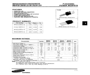
 4 Pages, 207 KB, Scan
fe operating area Improved high temperature reliability Rugged polysilicon gate cell structure TO-220 IRF9530/9531/9532/9533 TO-3P Part Number Vos Rosjon) lo IRF9530/RFP9130 -100V | 0.3002] -12A IRFO531/IRFP9131 | -6ov| 0300 | ~12A IRFP9190/9131/9132/9133 IRF9532/IRFP91 32 -100V | 0402] -10A IRF9533/IRFP9133 -60V | 0400 | -10A MAXIMUM RATINGS IRF9530 IRF9531 IRF9532 IRF9533 Characteristic Symbol IRF9130 7 IRF9131 IRFP9132 | IRFP9133 Unit Drain-Source Voltage {1) Voss -100 | -60 100 60 Vde Drain-Gate Voltage (Ras=1.0MM)(1) Vper 100 | 60 ~100 -60 Vdc Gate-Source Voltage Ves +20 Vde Continuous Drain Current Tc=25C Ib -12 -12 -10 -10 Adc Continuous Drain Current Tc= 100C fe) ~7.5 -7.5 -6.5 -6.5 Adc Drain CurrentPulsed (3) lom -48 48 -40 -40 Adc Gate CurrentPulsed lam #1.5 Adc Single Pulsed Avalanche Energy (4) Eas 550 mJ Avalanche Current las -12 A Total Power Dissipation @ Tc=25C Pp 75 Watts Derate above 25C 0.6 wiec Operating and Storage _ Junction Temperature Range Ta, Tstg 55 to 150
 6 Pages, 379 KB, Scan
00039 03038 02883 02883 02883 02883 03038 02883 02883 03038 03038 03038 03038 02037 02883 03038 02037 02037 01921 02883 02037 02037 JEDEC IRF9530 IRF130 M10N35 MTP2N90 2N5397 IRF9531 IRFD9120 IRFD110 IRF630 2N5912 IRF150 IRF9520 IRF830 RCA9212A MP833-1004 IRF9532 IRFD110 U311 IRFD113 IRFF210 IRFD9120 BUZ15 IRF640 VN0300M VP0300M MTM2P50 PF5101 (SEL) U310 IRF120 40673 IT1750 IRF440 BUZ24 2N5115 (SEL) MTP12N06 VN10KE VN0104N3 BUZ71A IRF512 VP0300L (SEL) IRFD420 BUZ10 J304 (SEL) VN0300L VN2222L SD306 (SEL) VN10LE IRF510 IRF250 MTP12N20 RFP10N12 IRFD9123 BUZ71A N E71000 2S K523 2S K533 IRF523 U440 J175 2N6660 IRF123 IRF521 VN0300M VQ1001 P IRF523 IRF9521 IRF9513 IRF513 IRF540 (SEL) VQ1000J IRF533 MTN12N06 M PF960 RFLlN08L VN2222LL MTP5N40 MTP4N50 Part Num. 1855-0608 1855-0614 1855-0617 1855-0618 1855-0619 1855-0620 1855-0621 1855-0622 1855-0623 1855-0625 1855-0629 1855-0630 1855-0631 1855-0632 1855-0635 1855-0636 1855-0637 1855-0639 1855-0640 1855-0641 1855-0645 1855-0646 1855-0647 1855-0649 1855-065
 143 Pages, 17060 KB, Original
se | |-100] nA Ves= 20V loss Zero Gate Voltage | | 250 | pA | Vos=Max. Rating, Ves=OV Drain Current | |1000] yA | Vps=Max. RatingX0.8, Ves=OV, Tco=125C On-State Drain-Source Current (2) IRF9530/IRFP91 30 -12) _ A Voss 4.8V, Vas=10V IRF9531/IRFP9131 loion) IRF9532/IRFP9132 ~10 A IRF9533/IRFP9133 ~ | Static Drain-Source On-State Resistance (2) _ __ Rosion) | iRF9530/IRFP9130 |) | 03 | @ | Ves=10V, In=6.5A IRF9531/IRFP9131 IRF9532/IRFP9132 ~|loa4 | a | IRF9533/IRFP9133 , Ofs Forward Transconductance (2) 2.0! _ oO Vos<50V, Ip=-6.5A Ciss Input Capacitance |835) pF Coss | Output Capacitance |357) pF Ves=OV, Vos=25V, f=1.0MHz Ciss Reverse Transfer Capacitance | 94 _ pF taon) | Turn-On Delay Time |- 60 ns ; ; Vop= 0.5BVpss, Ilp>=-6.5A, Zo=500 & Rise Time | | | 149 | NS _| (MOSFET switching times are essentially tai) | Turn-Off Delay Time /| | 140] ns independent of operating temperature) tt Fall Time |]| | 140 | ns Total Gate Charge Qg : -|- 45 | nd (Gate-Source Plus Gate-Drain) Vas= 15V, Ip
 6 Pages, 188 KB, Scan
 IRF520 IRF523 IRF532 MTP12N10 IRF533 MTP12N06 IRF541 IRF542 IRF543 IRF612 IRF613 BUZ76A IRF620 IRF622 IRF623 MTP4N15 IRF632 MTP8N20 IRF633 MTP8N15 IRF642 IRF643 MTP15N15 IRF720 IRF721 IRF722 IRF723 IRF730 IRF731 IRF743 IRF822 IRF823 IRF832 IRF833 IRF9132 IRF9532 IRFP140 MTM3N40 MTM3N35 2SK411 MTM5N40 MTM5N35 MTM8N40 MTM8N35 MTM15N40 MTM15N35 MTM10N25 MTM2N45 MTM2N50 MTM4N50 MTM4N45 MTM7N45 MTM7N50 MTP4N08 MTP8N08 MTP5N05 MTP10N08 2SK424 MTP4N10 MTP8N10 MTP5N06 MTP10N10 MTP12N08 MTP10N05 MTP10N06 MTP12N05 MTP25N05 MTP20N08 MTP15N05 MTP2N18 IRF612 ECG67 MTP3N20 MTP3N18 MTP3N12 MTP25N06 MTP20N20 MTP15N06 MTP2N20 VN0340N5 BUZ60 MTP5N18 MTP5N20 MTP3N15 MTP4N12 MTP7N18 MTP7N20 MTP8N18 MTP7N12 MTP7N15 MTP8N12 MTP12N18 MTP10N12 MTP12N20 MTP10N15 MTP15N12 MTP3N40 MTP3N35 MTP2N40 MTP2N25 MTP5N40 MTP5N35 MTP10N25 MTP1N50 MTP1N45 MTP4N50 MTP4N45 MTM8P08 MTP8P08 MTH25N08 IRF730 MTP2N35 MTP2N50 MTP2N45 MTM8P10 MTP8P10 MTH25N10 IRFP151 IRFP242 IRFP253 IRFP342 IRFP343 IS1 IS5 IS08 IS010 IS18 IS020 IS28 IS38 IS4
 314 Pages, 275 KB, Original
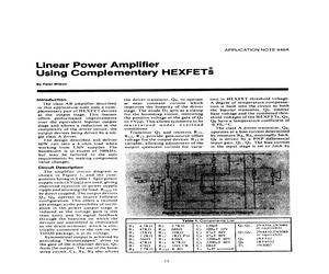
N] Riz [KO Pot. |] C4 Rs 5600 Ri3 8200 Cs Re 47K | Rig 4.7K0 Ce Ry 4709 Ris lOO 1W Cr Rg 2.7KQ.] Rioaad 8/42 Ly 220pF Q1.Q2, 2N4356,2N5086 100uF 10V or equivalent 47uF 40V Q3.Q4a, 2N4410,2N5088 47uF 40V or equivalent 2200nF 40V | Qs IRF532 2200uF 40V | Qs IRF9532 68nF Di 1N4002 3H aircoredresistor R3. Negative feedback from the output of the amplifier is fed to the base of Q2 by resistor Re. Com- ponents R7, C2 set the closed loop gain of the amplifier (Rg /R7) and provide low frequency gain boosting. The additional components R15, C7 connected between the output node and ground suppress the high fre- quency response of the output stage, allowing the h.f. performance of the amplifier to be determined by the input circuit. Components Rj, Ro, C, at the input of the amplifier define the input impedance (47Kohm) and suppress noise. The amplifier input stage requires additional power supply ripple sup- pression which is provided by com- ponents Ra, C3. Additional circuit components have been added to
 5 Pages, 882 KB, Scan
F9232 200 1.2 TO-3 _ ~~ = IRF9233 150 1.2 TO-3 _ _ _ IRF9520 100 0.6 TO-220 IRF9520* _ IRF9521 60 0.6 TO-220 IRF9521 aol IRF9522 100 0.8 TO-220 IRF9522 _ IRF9523 60 0.8 TO-220 IRE9523 _ _ IRF9530 100 0.3 TO-220 IRF9530* _ IRF9531 60 0.3 TO-220 IRF9531 _ _ IRF9532 100 0.4 TO-220 IRF9532 _ _ IRF9533 60 0.4 TO-220 (IRF9533 _ _ IRF9610 200 3.0 TO-220 _ _ (RF9611 150 3.0 TO-220 _ _ _ IRF9612 200 4.5 TO-220 _ _ _ IRF9613 150 4.5 TO-220 _ _ _ IRF9620 200 1.5 TO-220. _ _ ~ IRF9621 150 1.5 TO-220 _ _- _, IRF9622 200 24 TO-220 _ _ _ IRF9623 150 2.4 TO-220 _ _ : IRF9630 200 0.8 TO-220 _ _ _ \RF9631 150 0.8 TO-220 _ _ _ IRF9632 200 1.2 TO-220 _ _ _ (RF9633 150 1.2 TOQ-220 ~_ _ _ {RFF110 100 0.6 TO-39 _ ad IRFF111 60 0.6 TO-39 _ _ _ IRFF112 100 0.8 TO-39 _- - =_ IRFF113 60 0.8 TO-~39 - _ (RFF120 100 0.30 TO-39 IRFF120 _ _ IRFF121 60 0.30 TO-39 IRFF121 _ IRFF122 100 0.40 TO-39 IRFF122 - _ IRFF123 60 0.40 TO-39 IRFF123 _ _ IRFF130 100 0.18 TO-39 _ _ _ IRFF131 60 0.18 TO-39 _ _ > IRFF132 100 0.25 TO
 5 Pages, 192 KB, Scan


