25DCKR SN74LVC1G125DCKR 5 6 5 5 5 5 1G126 NC7S126M5 SN74AHC1G126DBVR 5 1G126 1G126 1G126 1G126 1G126 1G126 1G14 NC7S126M5X NC7SZ126L6X NC7SZ126M5 NC7SZ126M5X NC7SZ126P5 NC7SZ126P5X NC7S14L6X SN74AHC1G126DBVR Not available SN74LVC1G126DBVR SN74LVC1G126DBVR SN74LVC1G126DCKR SN74LVC1G126DCKR Not available 5 6 5 5 5 5 6 1G14 NC7S14M5 SN74AHC1G14DBVR 5 1G14 NC7S14M5X SN74AHC1G14DBVR 5 1G14 NC7S14P5 SN74AHC1G14DCKR 5 1G14 1G14 1G14 1G14 1G14 1G157 1G175 1G175 1G18 1G19 1G27 1G27 NC7S14P5X NC7SZ14M5 NC7SZ14M5X NC7SZ14P5 NC7SZ14P5X NC7SZ157P6X NC7SZ175P6 NC7SZ175P6X NC7SZ18P6X NC7SZ19P6X NC7SZ27P6 NC7SZ27P6X SN74AHC1G14DCKR SN74LVC1G14DBVR SN74LVC1G14DBVR SN74LVC1G14DCKR SN74LVC1G14DCKR Not available Not available Not available SN74LVC1G18DCKR SN74LVC1G19DCKR Not available Not available 5 5 5 5 5 6 6 6 6 6 6 6 1G3157 FSA3157L6X 1G3157 FSA3157P6X 1G3157 FSAU3157L6X 1G3157 FSAU3157P6X 1G3157 NC7SB3157L6X Not available SN74LVC1G3157DCKR Not available Not available 6 6 NC7SB3157P6X NC7SBU3157L6X
 329 Pages, 2106 KB, Original
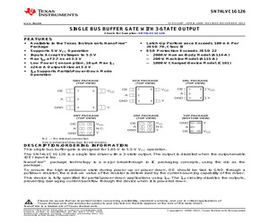
1) TA -40C to 85C ORDERABLE PART NUMBER NanoFreeTM - WCSP (DSBGA) 0.23-mm Large Bump - YZP (Pb-free) Reel of 3000 SN74LVC1G126YZPR _ _ _CN_ SON - DRY Reel of 5000 SN74LVC1G126DRYR CN_ Reel of 3000 SN74LVC1G126DBVR Reel of 250 SN74LVC1G126DBVT Reel of 3000 SN74LVC1G126DCKR Reel of 250 SN74LVC1G126DCKT Reel of 4000 SN74LVC1G126DRLR SOT (SOT-23) - DBV SOT (SC-70) - DCK SOT (SOT-553) - DRL (1) (2) C26_ CN_ CN_ Package drawings, standard packing quantities, thermal data, symbolization, and PCB design guidelines are available at www.ti.com/sc/package. DBV/DCK/DRL/DRY: The actual top-side marking has one additional character that designates the assembly/test site. YZP: The actual top-side marking has three preceding characters to denote year, month, and sequence code, and one following character to designate the assembly/test site. Pin 1 identifier indicates solder-bump composition (1 = SnPb, * = Pb-free). FUNCTION TABLE INPUTS OE A OUTPUT Y H H H H L L L X Z LOGIC DIAGRAM (POSITIVE LOGIC) 1 OE A 2 TOP-
 21 Pages, 802 KB, Original
1) TA -40C to 85C ORDERABLE PART NUMBER NanoFreeTM - WCSP (DSBGA) 0.23-mm Large Bump - YZP (Pb-free) Reel of 3000 SN74LVC1G126YZPR _ _ _CN_ SON - DRY Reel of 5000 SN74LVC1G126DRYR CN_ Reel of 3000 SN74LVC1G126DBVR Reel of 250 SN74LVC1G126DBVT Reel of 3000 SN74LVC1G126DCKR Reel of 250 SN74LVC1G126DCKT Reel of 4000 SN74LVC1G126DRLR SOT (SOT-23) - DBV SOT (SC-70) - DCK SOT (SOT-553) - DRL (1) (2) C26_ CN_ CN_ Package drawings, standard packing quantities, thermal data, symbolization, and PCB design guidelines are available at www.ti.com/sc/package. DBV/DCK/DRL/DRY: The actual top-side marking has one additional character that designates the assembly/test site. YZP: The actual top-side marking has three preceding characters to denote year, month, and sequence code, and one following character to designate the assembly/test site. Pin 1 identifier indicates solder-bump composition (1 = SnPb, * = Pb-free). FUNCTION TABLE INPUTS OE A OUTPUT Y H H H H L L L X Z LOGIC DIAGRAM (POSITIVE LOGIC) 1 OE A 2 TOP-
 21 Pages, 806 KB, Original
anoFreeTM - WCSP (DSBGA) 0.23-mm Large Bump - YZP (Pbfree) Reel of 3000 SN74LVC1G126YZPR _ _ _CN_ SON - DRY Reel of 5000 SN74LVC1G126DRYR CN QFN - DSF Reel of 5000 SN74LVC1G126DSFR CN Reel of 3000 SN74LVC1G126DBVR Reel of 250 SN74LVC1G126DBVT Reel of 3000 SN74LVC1G126DCKR Reel of 250 SN74LVC1G126DCKT Reel of 4000 SN74LVC1G126DRLR -40C to 85C SOT (SOT-23) - DBV SOT (SC-70) - DCK SOT (SOT-553) - DRL (1) (2) TOP-SIDE MARKING (2) C26_ CN_ CN_ Package drawings, standard packing quantities, thermal data, symbolization, and PCB design guidelines are available at www.ti.com/sc/package. DBV/DCK/DRL/DRY: The actual top-side marking has one additional character that designates the assembly/test site. YZP: The actual top-side marking has three preceding characters to denote year, month, and sequence code, and one following character to designate the assembly/test site. Pin 1 identifier indicates solder-bump composition (1 = SnPb, * = Pb-free). FUNCTION TABLE INPUTS OE A OUTPUT Y H H H H L L L X Z LOGIC DIAGR
 25 Pages, 1007 KB, Original
1) TA -40C to 85C ORDERABLE PART NUMBER NanoFreeTM - WCSP (DSBGA) 0.23-mm Large Bump - YZP (Pb-free) Reel of 3000 SN74LVC1G126YZPR _ _ _CN_ SON - DRY Reel of 5000 SN74LVC1G126DRYR CN_ Reel of 3000 SN74LVC1G126DBVR Reel of 250 SN74LVC1G126DBVT Reel of 3000 SN74LVC1G126DCKR Reel of 250 SN74LVC1G126DCKT Reel of 4000 SN74LVC1G126DRLR SOT (SOT-23) - DBV SOT (SC-70) - DCK SOT (SOT-553) - DRL (1) (2) C26_ CN_ CN_ Package drawings, standard packing quantities, thermal data, symbolization, and PCB design guidelines are available at www.ti.com/sc/package. DBV/DCK/DRL/DRY: The actual top-side marking has one additional character that designates the assembly/test site. YZP: The actual top-side marking has three preceding characters to denote year, month, and sequence code, and one following character to designate the assembly/test site. Pin 1 identifier indicates solder-bump composition (1 = SnPb, * = Pb-free). FUNCTION TABLE INPUTS OE A OUTPUT Y H H H H L L L X Z LOGIC DIAGRAM (POSITIVE LOGIC) 1 OE A 2 TOP-
 21 Pages, 970 KB, Original
1) TA -40C to 85C ORDERABLE PART NUMBER NanoFreeTM - WCSP (DSBGA) 0.23-mm Large Bump - YZP (Pb-free) Reel of 3000 SN74LVC1G126YZPR _ _ _CN_ SON - DRY Reel of 5000 SN74LVC1G126DRYR CN_ Reel of 3000 SN74LVC1G126DBVR Reel of 250 SN74LVC1G126DBVT Reel of 3000 SN74LVC1G126DCKR Reel of 250 SN74LVC1G126DCKT Reel of 4000 SN74LVC1G126DRLR SOT (SOT-23) - DBV SOT (SC-70) - DCK SOT (SOT-553) - DRL (1) (2) C26_ CN_ CN_ Package drawings, standard packing quantities, thermal data, symbolization, and PCB design guidelines are available at www.ti.com/sc/package. DBV/DCK/DRL/DRY: The actual top-side marking has one additional character that designates the assembly/test site. YZP: The actual top-side marking has three preceding characters to denote year, month, and sequence code, and one following character to designate the assembly/test site. Pin 1 identifier indicates solder-bump composition (1 = SnPb, * = Pb-free). FUNCTION TABLE INPUTS OE A OUTPUT Y H H H H L L L X Z LOGIC DIAGRAM (POSITIVE LOGIC) 1 OE A 2 TOP-
 20 Pages, 890 KB, Original
1) TA -40C to 85C ORDERABLE PART NUMBER NanoFreeTM - WCSP (DSBGA) 0.23-mm Large Bump - YZP (Pb-free) Reel of 3000 SN74LVC1G126YZPR _ _ _CN_ SON - DRY Reel of 5000 SN74LVC1G126DRYR CN_ Reel of 3000 SN74LVC1G126DBVR Reel of 250 SN74LVC1G126DBVT Reel of 3000 SN74LVC1G126DCKR Reel of 250 SN74LVC1G126DCKT Reel of 4000 SN74LVC1G126DRLR SOT (SOT-23) - DBV SOT (SC-70) - DCK SOT (SOT-553) - DRL (1) (2) C26_ CN_ CN_ Package drawings, standard packing quantities, thermal data, symbolization, and PCB design guidelines are available at www.ti.com/sc/package. DBV/DCK/DRL/DRY: The actual top-side marking has one additional character that designates the assembly/test site. YZP: The actual top-side marking has three preceding characters to denote year, month, and sequence code, and one following character to designate the assembly/test site. Pin 1 identifier indicates solder-bump composition (1 = SnPb, * = Pb-free). FUNCTION TABLE INPUTS OE A OUTPUT Y H H H H L L L X Z LOGIC DIAGRAM (POSITIVE LOGIC) 1 OE A 2 TOP-
 17 Pages, 598 KB, Original
CKR DBVR DBVR 5 5 5 5 5 5 5 5 5 5 5 5 5 5 5 5 SN74LVC1G126 SN74LVC1G126 SN74LVC1G126 SN74LVC1G126 SN74LVC1G126 SN74LVC1G126 SN74AHC1G126 SN74AHC1G126 SN74AHCT1G126 SN74AHCT1G126 SN74LVC1G126 SN74AHC1G126 SN74AHC1G126 SN74AHC1G126 SN74AHC1G126 SN74AHC1G126 SN74LVC1G126DCKR SN74LVC1G126DBVR SN74LVC1G126DCKR SN74LVC1G126DCKR SN74LVC1G126DCKR SN74LVC1G126DBVR SN74AHC1G126DCKR SN74AHC1G126DBVR SN74AHCT1G126DCKR SN74AHCT1G126DBVR SN74LVC1G126DCKR SN74AHC1G126DCKR SN74AHC1G126DCKR SN74AHC1G126DCKR SN74AHC1G126DBVR SN74AHC1G126DBVR IDT Philips Philips Philips STM STM STM STM STM STM IDT ON Semi ON Semi ON Semi ON Semi ON Semi LVC LVC LVC LVC LX1G LX1G 74V1G 74V1G 74V1T 74V1T LVC VHC VHC VHC VHC VHC -40 to 125C -40 to 125C -40 to 125C -55 to 125C -55 to 125C -55 to 125C -55 to 125C A-156 TI Comments -40 to 85C Faster, slightly lower max Vcc, not available in tubes, use DBVR Faster, slightly lower max Vcc This package Not available in tubes, use DBVR Not
 335 Pages, 1395 KB, Original
H16501DGGR SN74ALVCH16501DGGR SN74ALVCH16601DGGR SN74ALVCH16601DGGR SN74ALVCH16721DGGR SN74ALVCH16721DGGR SN74ALVCH16821DGGR SN74ALVCH16821DGGR SN74ALVCH16827DGGR SN74ALVCH16827DGGR SN74ALVC16835DGGR SN74ALVC16835DGGR SN74ALVCH16841DGGR SN74ALVCH16841DGGR SN74LVC1G126DCKR SN74ALVC244DWR SN74ALVC244PWR SN74ALVC244DW SN74ALVC32D SN74ALVC32PW SN74ALVC32PWR SN74ALVC32DR SN74ALVCF162835GR SN74ALVCF162835GR SN74ALVCH16244DL SN74ALVCH162244GR SN74ALVCH162244GR SN74ALVCH162244GR SN74ALVCH162244GR SN74ALVCH162244DL SN74ALVCH162244DLR SN74ALVCH162244DL SN74ALVCH162244DLR SN74ALVCH162244GR SN74ALVCH162244GR SN74ALVCH162244GR Replacement Code Q Q Q Q S S S Q Q Q Q Q Q S S S S Q Q Q Q Q Q Q Q Q Q Q Q S S Q Q Q S S S S S S S S S S S S S S S S S S S S S Competitor Fairchild Semiconductor Fairchild Semiconductor Fairchild Semiconductor Fairchild Semiconductor NXP Semiconductor Integrated Device Technology (IDT) Integrated Device Technology (IDT) Fairchild Semiconductor Fairchild Semiconductor Fairchild Semicondu
 441 Pages, 3298 KB, Original
25DCKR SN74LVC1G125DCKR 5 6 5 5 5 5 1G126 NC7S126M5 SN74AHC1G126DBVR 5 1G126 1G126 1G126 1G126 1G126 1G126 1G14 NC7S126M5X NC7SZ126L6X NC7SZ126M5 NC7SZ126M5X NC7SZ126P5 NC7SZ126P5X NC7S14L6X SN74AHC1G126DBVR Not available SN74LVC1G126DBVR SN74LVC1G126DBVR SN74LVC1G126DCKR SN74LVC1G126DCKR Not available 5 6 5 5 5 5 6 1G14 NC7S14M5 SN74AHC1G14DBVR 5 1G14 NC7S14M5X SN74AHC1G14DBVR 5 1G14 NC7S14P5 SN74AHC1G14DCKR 5 1G14 1G14 1G14 1G14 1G14 1G157 1G175 1G175 1G18 1G19 1G27 1G27 NC7S14P5X NC7SZ14M5 NC7SZ14M5X NC7SZ14P5 NC7SZ14P5X NC7SZ157P6X NC7SZ175P6 NC7SZ175P6X NC7SZ18P6X NC7SZ19P6X NC7SZ27P6 NC7SZ27P6X SN74AHC1G14DCKR SN74LVC1G14DBVR SN74LVC1G14DBVR SN74LVC1G14DCKR SN74LVC1G14DCKR Not available Not available Not available SN74LVC1G18DCKR SN74LVC1G19DCKR Not available Not available 5 5 5 5 5 6 6 6 6 6 6 6 1G3157 FSA3157L6X 1G3157 FSA3157P6X 1G3157 FSAU3157L6X 1G3157 FSAU3157P6X 1G3157 NC7SB3157L6X Not available SN74LVC1G3157DCKR Not available Not available 6 6 NC7SB3157P6X NC7SBU3157L6X
 379 Pages, 3043 KB, Original
25DCKR SN74LVC1G125DCKR 5 6 5 5 5 5 1G126 NC7S126M5 SN74AHC1G126DBVR 5 1G126 1G126 1G126 1G126 1G126 1G126 1G14 NC7S126M5X NC7SZ126L6X NC7SZ126M5 NC7SZ126M5X NC7SZ126P5 NC7SZ126P5X NC7S14L6X SN74AHC1G126DBVR Not available SN74LVC1G126DBVR SN74LVC1G126DBVR SN74LVC1G126DCKR SN74LVC1G126DCKR Not available 5 6 5 5 5 5 6 1G14 NC7S14M5 SN74AHC1G14DBVR 5 1G14 NC7S14M5X SN74AHC1G14DBVR 5 1G14 NC7S14P5 SN74AHC1G14DCKR 5 1G14 1G14 1G14 1G14 1G14 1G157 1G175 1G175 1G18 1G19 1G27 1G27 NC7S14P5X NC7SZ14M5 NC7SZ14M5X NC7SZ14P5 NC7SZ14P5X NC7SZ157P6X NC7SZ175P6 NC7SZ175P6X NC7SZ18P6X NC7SZ19P6X NC7SZ27P6 NC7SZ27P6X SN74AHC1G14DCKR SN74LVC1G14DBVR SN74LVC1G14DBVR SN74LVC1G14DCKR SN74LVC1G14DCKR Not available Not available Not available SN74LVC1G18DCKR SN74LVC1G19DCKR Not available Not available 5 5 5 5 5 6 6 6 6 6 6 6 1G3157 FSA3157L6X 1G3157 FSA3157P6X 1G3157 FSAU3157L6X 1G3157 FSAU3157P6X 1G3157 NC7SB3157L6X Not available SN74LVC1G3157DCKR Not available Not available 6 6 NC7SB3157P6X NC7SBU3157L6X
 313 Pages, 2889 KB, Original
1) TA -40C to 85C ORDERABLE PART NUMBER NanoFreeTM - WCSP (DSBGA) 0.23-mm Large Bump - YZP (Pb-free) Reel of 3000 SN74LVC1G126YZPR _ _ _CN_ SON - DRY Reel of 5000 SN74LVC1G126DRYR CN_ Reel of 3000 SN74LVC1G126DBVR Reel of 250 SN74LVC1G126DBVT Reel of 3000 SN74LVC1G126DCKR Reel of 250 SN74LVC1G126DCKT Reel of 4000 SN74LVC1G126DRLR SOT (SOT-23) - DBV SOT (SC-70) - DCK SOT (SOT-553) - DRL (1) (2) C26_ CN_ CN_ Package drawings, standard packing quantities, thermal data, symbolization, and PCB design guidelines are available at www.ti.com/sc/package. DBV/DCK/DRL/DRY: The actual top-side marking has one additional character that designates the assembly/test site. YZP: The actual top-side marking has three preceding characters to denote year, month, and sequence code, and one following character to designate the assembly/test site. Pin 1 identifier indicates solder-bump composition (1 = SnPb, * = Pb-free). FUNCTION TABLE INPUTS OE A OUTPUT Y H H H H L L L X Z LOGIC DIAGRAM (POSITIVE LOGIC) 1 OE A 2 TOP-
 19 Pages, 829 KB, Original
1) TA -40C to 85C ORDERABLE PART NUMBER NanoFreeTM - WCSP (DSBGA) 0.23-mm Large Bump - YZP (Pb-free) Reel of 3000 SN74LVC1G126YZPR _ _ _CN_ SON - DRY Reel of 5000 SN74LVC1G126DRYR CN_ Reel of 3000 SN74LVC1G126DBVR Reel of 250 SN74LVC1G126DBVT Reel of 3000 SN74LVC1G126DCKR Reel of 250 SN74LVC1G126DCKT Reel of 4000 SN74LVC1G126DRLR SOT (SOT-23) - DBV SOT (SC-70) - DCK SOT (SOT-553) - DRL (1) (2) C26_ CN_ CN_ Package drawings, standard packing quantities, thermal data, symbolization, and PCB design guidelines are available at www.ti.com/sc/package. DBV/DCK/DRL/DRY: The actual top-side marking has one additional character that designates the assembly/test site. YZP: The actual top-side marking has three preceding characters to denote year, month, and sequence code, and one following character to designate the assembly/test site. Pin 1 identifier indicates solder-bump composition (1 = SnPb, * = Pb-free). FUNCTION TABLE INPUTS OE A OUTPUT Y H H H H L L L X Z LOGIC DIAGRAM (POSITIVE LOGIC) 1 OE A 2 TOP-
 17 Pages, 563 KB, Original
1) TA -40C to 85C ORDERABLE PART NUMBER NanoFreeTM - WCSP (DSBGA) 0.23-mm Large Bump - YZP (Pb-free) Reel of 3000 SN74LVC1G126YZPR _ _ _CN_ SON - DRY Reel of 5000 SN74LVC1G126DRYR CN_ Reel of 3000 SN74LVC1G126DBVR Reel of 250 SN74LVC1G126DBVT Reel of 3000 SN74LVC1G126DCKR Reel of 250 SN74LVC1G126DCKT Reel of 4000 SN74LVC1G126DRLR SOT (SOT-23) - DBV SOT (SC-70) - DCK SOT (SOT-553) - DRL (1) (2) C26_ CN_ CN_ Package drawings, standard packing quantities, thermal data, symbolization, and PCB design guidelines are available at www.ti.com/sc/package. DBV/DCK/DRL/DRY: The actual top-side marking has one additional character that designates the assembly/test site. YZP: The actual top-side marking has three preceding characters to denote year, month, and sequence code, and one following character to designate the assembly/test site. Pin 1 identifier indicates solder-bump composition (1 = SnPb, * = Pb-free). FUNCTION TABLE INPUTS OE A OUTPUT Y H H H H L L L X Z LOGIC DIAGRAM (POSITIVE LOGIC) 1 OE A 2 TOP-
 17 Pages, 600 KB, Original
anoFreeTM - WCSP (DSBGA) 0.23-mm Large Bump - YZP (Pbfree) Reel of 3000 SN74LVC1G126YZPR _ _ _CN_ SON - DRY Reel of 5000 SN74LVC1G126DRYR CN QFN - DSF Reel of 5000 SN74LVC1G126DSFR CN Reel of 3000 SN74LVC1G126DBVR Reel of 250 SN74LVC1G126DBVT Reel of 3000 SN74LVC1G126DCKR Reel of 250 SN74LVC1G126DCKT Jumbo Reel of 10000 SN74LVC1G126DCKJ Reel of 4000 SN74LVC1G126DRLR SOT (SOT-23) - DBV SOT (SC-70) - DCK SOT (SOT-553) - DRL (1) (2) TOP-SIDE MARKING (2) C26_ CN_ CN_ Package drawings, standard packing quantities, thermal data, symbolization, and PCB design guidelines are available at www.ti.com/sc/package. DBV/DCK/DRL/DRY: The actual top-side marking has one additional character that designates the assembly/test site. YZP: The actual top-side marking has three preceding characters to denote year, month, and sequence code, and one following character to designate the assembly/test site. Pin 1 identifier indicates solder-bump composition (1 = SnPb, * = Pb-free). FUNCTION TABLE INPUTS OE A OUTPUT Y H H
 25 Pages, 1211 KB, Original


