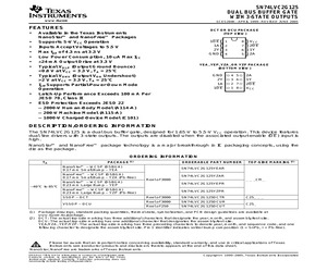
- WCSP (DSBGA) 0.23-mm Large Bump - YEP SN74LVC2G125YEAR SN74LVC2G125YZAR Reel of 3000 VSSOP - DCU (1) (2) _ _ _CM_ SN74LVC2G125YEPR NanoFreeTM - WCSP (DSBGA) 0.23-mm Large Bump - YZP (Pb-free) SSOP - DCT TOP-SIDE MARKING (2) SN74LVC2G125YZPR Reel of 3000 SN74LVC2G125DCTR Reel of 3000 SN74LVC2G125DCUR Reel of 250 SN74LVC2G125DCUT C25_ _ _ C25_ Package drawings, standard packing quantities, thermal data, symbolization, and PCB design guidelines are available at www.ti.com/sc/package. DCT: The actual top-side marking has three additional characters that designate the year, month, and assembly/test site. DCU: The actual top-side marking has one additional character that designates the assembly/test site. YEA/YZA, YEP/YZP: The actual top-side marking has three preceding characters to denote year, month, and sequence code, and one following character to designate the assembly/test site. Pin 1 identifier indicates solder-bump composition (1 = SnPb, * = Pb-free). Please be aware that an important notice
 18 Pages, 542 KB, Original
- WCSP (DSBGA) 0.23-mm Large Bump - YEP SN74LVC2G125YEAR SN74LVC2G125YZAR Reel of 3000 VSSOP - DCU (1) (2) _ _ _CM_ SN74LVC2G125YEPR NanoFreeTM - WCSP (DSBGA) 0.23-mm Large Bump - YZP (Pb-free) SSOP - DCT TOP-SIDE MARKING (2) SN74LVC2G125YZPR Reel of 3000 SN74LVC2G125DCTR Reel of 3000 SN74LVC2G125DCUR Reel of 250 SN74LVC2G125DCUT C25_ _ _ C25_ Package drawings, standard packing quantities, thermal data, symbolization, and PCB design guidelines are available at www.ti.com/sc/package. DCT: The actual top-side marking has three additional characters that designate the year, month, and assembly/test site. DCU: The actual top-side marking has one additional character that designates the assembly/test site. YEA/YZA, YEP/YZP: The actual top-side marking has three preceding characters to denote year, month, and sequence code, and one following character to designate the assembly/test site. Pin 1 identifier indicates solder-bump composition (1 = SnPb, * = Pb-free). Please be aware that an important notice
 19 Pages, 612 KB, Original
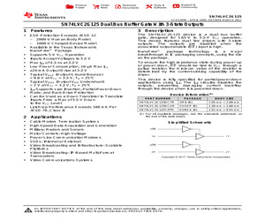
r. This device is fully specified for partial-power-down applications using Ioff. The Ioff circuitry disables the outputs, preventing damaging current backflow through the device when it is powered down. Device Information(1) PART NUMBER PACKAGE BODY SIZE SN74LVC2G125DCTR SM8 (8) 2.95 mm x 2.80 mm SN74LVC2G125DCUR VSSOP (8) 2.30 mm x 2.00 mm SN74LVC2G125YZPR DSBGA (8) 1.91 mm x 0.91 mm (1) For all available packages, see the orderable addendum at the end of the data sheet. Simplified Schematic 1 OE 1A 1Y 2 OE 2A 2Y Copyright (c) 2017, Texas Instruments Incorporated 1 An IMPORTANT NOTICE at the end of this data sheet addresses availability, warranty, changes, use in safety-critical applications, intellectual property matters and other important disclaimers. PRODUCTION DATA. SN74LVC2G125 SCES204Q - APRIL 1999 - REVISED MARCH 2017 www.ti.com Table of Contents 1 2 3 4 5 6 7 8 Features .................................................................. Applications .....................................
 28 Pages, 1049 KB, Original
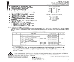
rrent backflow through the device when it is powered down. ORDERING INFORMATION PACKAGE (1) TA -40C to 85C (2) TOP-SIDE MARKING (2) NanoFreeTM - WCSP (DSBGA) 0.23-mm Large Bump - YZP (Pb-free) Reel of 3000 SN74LVC2G125YZPR _ _ _CM_ SSOP - DCT Reel of 3000 SN74LVC2G125DCTR C25_ _ _ Reel of 3000 SN74LVC2G125DCUR Reel of 250 SN74LVC2G125DCUT VSSOP - DCU (1) ORDERABLE PART NUMBER C25_ Package drawings, standard packing quantities, thermal data, symbolization, and PCB design guidelines are available at www.ti.com/sc/package. DCT: The actual top-side marking has three additional characters that designate the year, month, and assembly/test site. DCU: The actual top-side marking has one additional character that designates the assembly/test site. YZP: The actual top-side marking has three preceding characters to denote year, month, and sequence code, and one following character to designate the assembly/test site. Pin 1 identifier indicates solder-bump composition (1 = SnPb, * = Pb-free). Please be aware
 13 Pages, 420 KB, Original
(Pb-free) -40C to 85C NanoStar - WCSP (DSBGA) 0.23-mm Large Bump - YEP SN74LVC2G125YZAR Reel of 3000 VSSOP - DCU _ _ _CM_ SN74LVC2G125YEPR NanoFree - WCSP (DSBGA) 0.23-mm Large Bump - YZP (Pb-free) SSOP - DCT TOP-SIDE MARKING SN74LVC2G125YZPR Reel of 3000 SN74LVC2G125DCTR Reel of 3000 SN74LVC2G125DCUR Reel of 250 SN74LVC2G125DCUT C25_ _ _ C25_ Package drawings, standard packing quantities, thermal data, symbolization, and PCB design guidelines are available at www.ti.com/sc/package. DCT: The actual top-side marking has three additional characters that designate the year, month, and assembly/test site. DCU: The actual top-side marking has one additional character that designates the assembly/test site. YEA/YZA, YEP/YZP: The actual top-side marking has three preceding characters to denote year, month, and sequence code, and one following character to designate the assembly/test site. Pin 1 identifier indicates solder-bump composition (1 = SnPb, * = Pb-free). Please be aware that an important notice
 13 Pages, 332 KB, Original
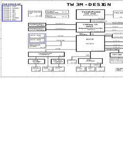
DS). +3VRUN DVI DETECT CRT_B_COM 7 R119 *1K R118 *1K +3VRUN NC7SB3157P6X_NL HIGH IN_B1 1 HSYNC_COM 2 1A 2OE# 7 PR_INSERT# 3 2Y 1Y 6 CRT_HSYNC 4 GND 2A 5 HSYNC_COM PR_HSYNC 35 PR_HSYNC +3VRUN 1 U4 INTVGA_E 35 PR_VSYNC DVI_DET R125 *10K 1 INTVGA_E 2 3 IN_B0 SN74LVC2G125DCTR 1OE# VCC 8 2 1 LOW C97 0.1u/10V CC0402 U1 FUNCTION(COM) 3 DVI_DETECT 18 +3VRUN SEL HSYNC_COM Q13 *MMBT3904 Q12 *MMBT3904 Install for DVI 7 +3VRUN SN74LVC2G125DCTR VCC 8 1 1OE# VSYNC_COM 2 1A 2OE# 7 PR_INSERT# PR_VSYNC 3 2Y 1Y 6 CRT_VSYNC 4 GND 2A 5 VSYNC_COM 1 C115 0.1u/10V CC0402 PROJECT : TW3 Quanta Computer Inc. VSYNC_COM 7 Size Document Number Rev B2A CRT,TV-OUT,DVI CONN. Date: A B C D Tuesday, January 03, 2006 Sheet E 23 of 46 5 4 3 2 1 24 C: 88E8053 LF PN: AJ080530010 (20050414) 1Mbits C: Add 9 X GND Pad for LAN controller. (20050411) D C: Add these GND pin for via hole to GND Plane. LANVCC C: Add RC (R37 change to 200K, Add C101) delay to control LOM_DISABLE#. (20050411) D 13 PCIE_TXP2 13 PCIE_TXN2 65 36 37 3
 47 Pages, 1144 KB, Original
rrent backflow through the device when it is powered down. ORDERING INFORMATION PACKAGE (1) TA -40C to 85C (2) TOP-SIDE MARKING (2) NanoFreeTM - WCSP (DSBGA) 0.23-mm Large Bump - YZP (Pb-free) Reel of 3000 SN74LVC2G125YZPR _ _ _CM_ SSOP - DCT Reel of 3000 SN74LVC2G125DCTR C25_ _ _ Reel of 3000 SN74LVC2G125DCUR Reel of 250 SN74LVC2G125DCUT VSSOP - DCU (1) ORDERABLE PART NUMBER C25_ Package drawings, standard packing quantities, thermal data, symbolization, and PCB design guidelines are available at www.ti.com/sc/package. DCT: The actual top-side marking has three additional characters that designate the year, month, and assembly/test site. DCU: The actual top-side marking has one additional character that designates the assembly/test site. YZP: The actual top-side marking has three preceding characters to denote year, month, and sequence code, and one following character to designate the assembly/test site. Pin 1 identifier indicates solder-bump composition (1 = SnPb, * = Pb-free). Please be aware
 15 Pages, 528 KB, Original
rrent backflow through the device when it is powered down. ORDERING INFORMATION PACKAGE (1) TA -40C to 85C (2) TOP-SIDE MARKING (2) NanoFreeTM - WCSP (DSBGA) 0.23-mm Large Bump - YZP (Pb-free) Reel of 3000 SN74LVC2G125YZPR _ _ _CM_ SSOP - DCT Reel of 3000 SN74LVC2G125DCTR C25_ _ _ Reel of 3000 SN74LVC2G125DCUR Reel of 250 SN74LVC2G125DCUT VSSOP - DCU (1) ORDERABLE PART NUMBER C25_ Package drawings, standard packing quantities, thermal data, symbolization, and PCB design guidelines are available at www.ti.com/sc/package. DCT: The actual top-side marking has three additional characters that designate the year, month, and assembly/test site. DCU: The actual top-side marking has one additional character that designates the assembly/test site. YZP: The actual top-side marking has three preceding characters to denote year, month, and sequence code, and one following character to designate the assembly/test site. Pin 1 identifier indicates solder-bump composition (1 = SnPb, * = Pb-free). Please be aware
 15 Pages, 722 KB, Original
SN74LVC2G04DCKR SN74LVC2G04DCKR SN74LVC2G06DBVR SN74LVC2G06DCKR SN74LVC2G06DCKR SN74LVC2G07DBVR SN74LVC2G07DCKR SN74LVC2G07DCKR Not available Not available Not available Not available SN74LVC2G08DCTR Not available Not available Not available Not available SN74LVC2G125DCTR Not available Not available Not available Not available SN74LVC2G126DCTR Not available Not available Not available Not available SN74LVC2G14DBVR SN74LVC2G14DCKR SN74LVC2G14DCKR SN74LVC2G17DBVR SN74LVC2G17DCKR SN74LVC2G17DCKR SN74LVC2G240DCTR SN74LVC2G241DCTR Not available Not available SN74LVC2G34DCKR 5 5 5 5 8 8 8 8 8 8 8 8 6 6 6 6 6 6 6 6 6 8 8 8 8 8 8 8 8 8 8 8 8 8 8 8 6 6 6 6 6 6 6 6 6 6 8 8 8 8 6 1G86 1G86 1G86 1G86 1GU04 1GU04 1GU04 74HC1GU04GW-G 74LVC1GU04GV 74LVC1GU04GW 74LVC1GU04GW-G 74HC2G00DC 74HC2G00DP 74HCT2G00DC 74HCT2G00DP 74HC2G02DC 74HC2G02DP 74HCT2G02DC 74HCT2G02DP 74LVC2G04GV 74LVC2G04GW 74LVC2G04GW-G 74LVC2G06GV 74LVC2G06GW 74LVC2G06GW-G 74LVC2G07GV 74LVC2G07GW 74LVC2G07GW-G 74HC2G08DC 74HC2G08DP 74HCT2G08DC
 313 Pages, 2889 KB, Original
to 125C Specs. similar to AHC -40 to 125C -40 to 125C -40 to 125C -40 to 125C -40 to 125C Specs. similar to AHC Specs. similar to AHC -40 to 125C -40 to 125C -40 to 125C A-162 SN74LVC2G08DCUR SN74LVC2G08DCUR SN74LVC2G00DCUR SN74LVC2G08DCUR SN74LVC2G08DCUR SN74LVC2G125DCTR SN74LVC2G125DCUR SN74LVC2G125DCUR SN74LVC2G126DCTR SN74LVC2G126DCUR SN74LVC2G126DCUR TI Comments Preview, faster, higher output drive, Ioff Consider LVC Little Logic Consider LVC Little Logic Consider LVC Little Logic Consider LVC Little Logic Consider LVC Little Logic Consider LVC Little Logic Not available in tubes, use reeled DCKR Consider LVC Little Logic Consider LVC Little Logic Consider LVC Little Logic Not available in tubes, use DCUR Faster, higher output drive, Ioff Consider LVC Little Logic Consider LVC Little Logic Consider LVC Little Logic Not available in tubes, use DCUR Consider LVC Little Logic Consider LVC Little Logic Consider LVC Little Logic Not available in tubes, use DCUR Consider LVC Little Logic Consider
 335 Pages, 1395 KB, Original
SN74LVC2G04DCKR SN74LVC2G04DCKR SN74LVC2G06DBVR SN74LVC2G06DCKR SN74LVC2G06DCKR SN74LVC2G07DBVR SN74LVC2G07DCKR SN74LVC2G07DCKR Not available Not available Not available Not available SN74LVC2G08DCTR Not available Not available Not available Not available SN74LVC2G125DCTR Not available Not available Not available Not available SN74LVC2G126DCTR Not available Not available Not available Not available SN74LVC2G14DBVR SN74LVC2G14DCKR SN74LVC2G14DCKR SN74LVC2G17DBVR SN74LVC2G17DCKR SN74LVC2G17DCKR SN74LVC2G240DCTR SN74LVC2G241DCTR Not available Not available SN74LVC2G34DCKR 5 5 5 5 8 8 8 8 8 8 8 8 6 6 6 6 6 6 6 6 6 8 8 8 8 8 8 8 8 8 8 8 8 8 8 8 6 6 6 6 6 6 6 6 6 6 8 8 8 8 6 1G86 1G86 1G86 1G86 1GU04 1GU04 1GU04 74HC1GU04GW-G 74LVC1GU04GV 74LVC1GU04GW 74LVC1GU04GW-G 74HC2G00DC 74HC2G00DP 74HCT2G00DC 74HCT2G00DP 74HC2G02DC 74HC2G02DP 74HCT2G02DC 74HCT2G02DP 74LVC2G04GV 74LVC2G04GW 74LVC2G04GW-G 74LVC2G06GV 74LVC2G06GW 74LVC2G06GW-G 74LVC2G07GV 74LVC2G07GW 74LVC2G07GW-G 74HC2G08DC 74HC2G08DP 74HCT2G08DC
 379 Pages, 3043 KB, Original
SN74LVC2G04DCKR SN74LVC2G04DCKR SN74LVC2G06DBVR SN74LVC2G06DCKR SN74LVC2G06DCKR SN74LVC2G07DBVR SN74LVC2G07DCKR SN74LVC2G07DCKR Not available Not available Not available Not available SN74LVC2G08DCTR Not available Not available Not available Not available SN74LVC2G125DCTR Not available Not available Not available Not available SN74LVC2G126DCTR Not available Not available Not available Not available SN74LVC2G14DBVR SN74LVC2G14DCKR SN74LVC2G14DCKR SN74LVC2G17DBVR SN74LVC2G17DCKR SN74LVC2G17DCKR SN74LVC2G240DCTR SN74LVC2G241DCTR Not available Not available SN74LVC2G34DCKR 5 5 5 5 8 8 8 8 8 8 8 8 6 6 6 6 6 6 6 6 6 8 8 8 8 8 8 8 8 8 8 8 8 8 8 8 6 6 6 6 6 6 6 6 6 6 8 8 8 8 6 1G86 1G86 1G86 1G86 1GU04 1GU04 1GU04 74HC1GU04GW-G 74LVC1GU04GV 74LVC1GU04GW 74LVC1GU04GW-G 74HC2G00DC 74HC2G00DP 74HCT2G00DC 74HCT2G00DP 74HC2G02DC 74HC2G02DP 74HCT2G02DC 74HCT2G02DP 74LVC2G04GV 74LVC2G04GW 74LVC2G04GW-G 74LVC2G06GV 74LVC2G06GW 74LVC2G06GW-G 74LVC2G07GV 74LVC2G07GW 74LVC2G07GW-G 74HC2G08DC 74HC2G08DP 74HCT2G08DC
 329 Pages, 2106 KB, Original
rrent backflow through the device when it is powered down. ORDERING INFORMATION PACKAGE (1) TA -40C to 85C (2) TOP-SIDE MARKING (2) NanoFreeTM - WCSP (DSBGA) 0.23-mm Large Bump - YZP (Pb-free) Reel of 3000 SN74LVC2G125YZPR _ _ _CM_ SSOP - DCT Reel of 3000 SN74LVC2G125DCTR C25_ _ _ Reel of 3000 SN74LVC2G125DCUR Reel of 250 SN74LVC2G125DCUT VSSOP - DCU (1) ORDERABLE PART NUMBER C25_ Package drawings, standard packing quantities, thermal data, symbolization, and PCB design guidelines are available at www.ti.com/sc/package. DCT: The actual top-side marking has three additional characters that designate the year, month, and assembly/test site. DCU: The actual top-side marking has one additional character that designates the assembly/test site. YZP: The actual top-side marking has three preceding characters to denote year, month, and sequence code, and one following character to designate the assembly/test site. Pin 1 identifier indicates solder-bump composition (1 = SnPb, * = Pb-free). Please be aware
 13 Pages, 426 KB, Original
(Pb-free) -40C to 85C NanoStar - WCSP (DSBGA) 0.23-mm Large Bump - YEP SN74LVC2G125YZAR Reel of 3000 VSSOP - DCU _ _ _CM_ SN74LVC2G125YEPR NanoFree - WCSP (DSBGA) 0.23-mm Large Bump - YZP (Pb-free) SSOP - DCT TOP-SIDE MARKING SN74LVC2G125YZPR Reel of 3000 SN74LVC2G125DCTR Reel of 3000 SN74LVC2G125DCUR Reel of 250 SN74LVC2G125DCUT C25_ _ _ C25_ Package drawings, standard packing quantities, thermal data, symbolization, and PCB design guidelines are available at www.ti.com/sc/package. DCT: The actual top-side marking has three additional characters that designate the year, month, and assembly/test site. DCU: The actual top-side marking has one additional character that designates the assembly/test site. YEA/YZA, YEP/YZP: The actual top-side marking has three preceding characters to denote year, month, and sequence code, and one following character to designate the assembly/test site. Pin 1 identifier indicates solder-bump composition (1 = SnPb, * = Pb-free). Please be aware that an important notice
 13 Pages, 328 KB, Original
rrent backflow through the device when it is powered down. ORDERING INFORMATION PACKAGE (1) TA -40C to 85C (2) TOP-SIDE MARKING (2) NanoFreeTM - WCSP (DSBGA) 0.23-mm Large Bump - YZP (Pb-free) Reel of 3000 SN74LVC2G125YZPR _ _ _CM_ SSOP - DCT Reel of 3000 SN74LVC2G125DCTR C25_ _ _ Reel of 3000 SN74LVC2G125DCUR Reel of 250 SN74LVC2G125DCUT VSSOP - DCU (1) ORDERABLE PART NUMBER C25_ Package drawings, standard packing quantities, thermal data, symbolization, and PCB design guidelines are available at www.ti.com/sc/package. DCT: The actual top-side marking has three additional characters that designate the year, month, and assembly/test site. DCU: The actual top-side marking has one additional character that designates the assembly/test site. YZP: The actual top-side marking has three preceding characters to denote year, month, and sequence code, and one following character to designate the assembly/test site. Pin 1 identifier indicates solder-bump composition (1 = SnPb, * = Pb-free). Please be aware
 15 Pages, 530 KB, Original


