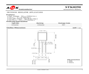
STK0250 Semiconductor Advanced Power MOSFET SWITCHING REGULATOR APPLICATIONS Features * * * * High Voltage : BVDSS=500V(Min.) Low Crss : Crss=6.5pF(Typ.) Low gate charge : Qg=8.5nC(Typ.) Low RDS(on) : RDS(on)=3.3(Max.) Ordering Information Type NO. Marking STK0250 Package Code STK0250 MPT Outline Dimensions unit : mm 8.40~8.60 7.30~7.50 1.70 Typ. 1.20 Max. 13.05~13.85 0.70 Max. 0.60 Max. 2.50 Typ. 2.50 Typ. 2 3 0.60 Max. 1.95~2.05 3.30~3.50 1 KSD-T0H007-002 PIN Connections 1. Gate 2. Drain 3. Source 1 STK0250 Absolute maximum ratings (Ta=25C) Characteristic Symbol Rating Unit Drain-source voltage VDSS 500 V Gate-source voltage VGSS 30 V Drain current (DC) ID 0.6 A * IDP 2.4 A Drain Power dissipation PD 1.3 W Drain current (Pulsed) Avalanche current (Single) IAS 0.6 A Single pulsed avalanche energy EAS 4.0 mJ Avalanche current (Repetitive) IAR 0.6 A Repetitive avalanche energy EAR 0.1 mJ TJ Tstg 150 -55~150 C Junction temperature Storage temperature range * L
 8 Pages, 458 KB, Original
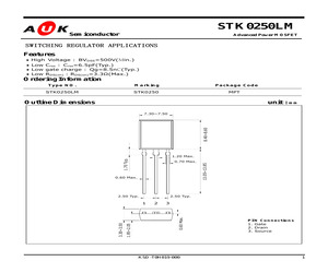
STK0250LM Semiconductor Advanced Power MOSFET SWITCHING REGULATOR APPLICATIONS Features * * * * High Voltage : BVDSS=500V(Min.) Low Crss : Crss=6.5pF(Typ.) Low gate charge : Qg=8.5nC(Typ.) Low RDS(on) : RDS(on)=3.3(Max.) Ordering Information Type NO. Marking STK0250LM STK0250 Package Code MPT Outline Dimensions unit : mm 8.40~8.60 7.30~7.50 1.70 Typ. 1.20 Max. 13.05~13.85 0.70 Max. 0.60 Max. 2.50 Typ. 2.50 Typ. 2 3 0.60 Max. 1.95~2.05 3.30~3.50 1 KSD-T0H019-000 PIN Connections 1. Gate 2. Drain 3. Source 1 STK0250LM Absolute maximum ratings (Ta=25C) Characteristic Symbol Rating Unit Drain-source voltage VDSS 500 V Gate-source voltage VGSS 30 V Drain current (DC) ID 0.64 A * IDP 2.4 A Drain Power dissipation PD 1.3 W Drain current (Pulsed) Avalanche current (Single) IAS 0.6 A Single pulsed avalanche energy EAS 4.0 mJ Avalanche current (Repetitive) IAR 0.6 A Repetitive avalanche energy EAR 0.1 mJ TJ Tstg 150 -55~150 C Junction temperature Storage temperature ra
 8 Pages, 365 KB, Original
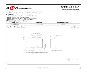
STK0250D Semiconductor Advanced Power MOSFET SWITCHING REGULATOR APPLICATIONS Features * * * * High Voltage : BVDSS=500V(Min.) Low Crss : Crss=6.5pF(Typ.) Low gate charge : Qg=8.5nC(Typ.) Low RDS(on) : RDS(on)=3.3(Max.) Ordering Information Type NO. Marking STK0250D Package Code STK0250 D-PAK Outline Dimensions unit : mm 6.50~6.70 5.10~5.50 1.15 Max. 7.77~7.97 1.18 Max. 2.10~2.50 0.55 Max. 0.83 Max. 2.30 Typ. 2.30 Typ. 1 2 3 PIN Connections 1. Gate 2. Drain 3. Source KSD-T6O001-000 1 STK0250D Absolute maximum ratings (Tc=25C) Characteristic Symbol Rating Unit Drain-source voltage VDSS 500 V Gate-source voltage VGSS 30 V (Tc=25) 2.0 A (Tc=125) 1.7 A * IDP 8.0 A Drain Power dissipation PD 35 W Drain current (DC) ID Drain current (Pulsed) Avalanche current (Single) IAS 2.0 A Single pulsed avalanche energy EAS 59 mJ Avalanche current (Repetitive) IAR 2.0 A Repetitive avalanche energy EAR 3.0 mJ TJ Tstg 150 -55~150 C Junction temperature Storage temperature range
 8 Pages, 453 KB, Original
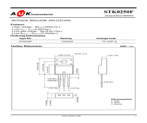
STK0250F Semiconductor Advanced Power MOSFET SWITCHING REGULATOR APPLICATIONS Features * * * * High Voltage : BVDSS=500V(Min.) Low Crss : Crss=6.5pF(Typ.) Low gate charge : Qg=8.5nC(Typ.) Low RDS(on) : RDS(on)=3.3(Max.) Ordering Information Type NO. Marking STK0250F Package Code STK0250 TO-220F-3L Outline Dimensions unit : mm 3.46 Typ. 9.10~9.30 2.60~3.00 0.90 Max. 0.60 Max. 2.54 Typ. 2.54 Typ. 2 3 0.60 Max. 1 2.70 Max. 12.20~12.60 3.05~3.35 1.07 Min. 4.70 Max. 15.40~15.80 9.80~10.20 KSD-T0O012-000 PIN Connections 1. Gate 2. Drain 3. Source 1 STK0250F Absolute maximum ratings (Tc=25C) Characteristic Symbol Rating Unit Drain-source voltage VDSS 500 V Gate-source voltage VGSS 30 V (Tc=25) 2.0 A (Tc=100) 1.7 A * IDP 8.0 A Drain Power dissipation PD 22 W Drain current (DC) ID Drain current (Pulsed) Avalanche current (Single) IAS 2.0 A Single pulsed avalanche energy EAS 59 mJ Avalanche current (Repetitive) IAR 2.0 A Repetitive avalanche energy EAR 3.0 mJ TJ Tstg
 8 Pages, 459 KB, Original
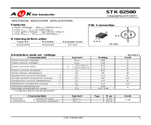
STK0250D Semiconductor Advanced Power MOSFET SWITCHING REGULATOR APPLICATIONS Features * * * * PIN Connection High Voltage : BVDSS=500V(Min.) Low Crss : Crss=6.5pF(Typ.) Low gate charge : Qg=8.5nC(Typ.) Low RDS(on) : RDS(on)=3.3(Max.) D D G Ordering Information Type No. Marking Package Code STK0250D STK0250 TO-252 GDS S TO-252 Absolute maximum ratings (Tc=25C) Characteristic Symbol Rating Unit Drain-source voltage VDSS 500 V Gate-source voltage VGSS 30 V (Tc=25) 2.0 A Drain current (DC) ID (Tc=125) 1.7 A * IDP 8.0 A Drain Power dissipation PD 35 W Drain current (Pulsed) Avalanche current (Single) IAS 2.0 A Single pulsed avalanche energy EAS 59 mJ Avalanche current (Repetitive) IAR 2.0 A Repetitive avalanche energy EAR 3.0 mJ TJ Tstg 150 -55~150 C Junction temperature Storage temperature range * Limited by maximum junction temperature Characteristic Thermal resistance Symbol Typ. Max Junction-case Rth(J-C) - 3.57 Junction-ambient Rth(J-a) - 62.5 KSD-T6O001-001 Unit /W 1 <
 8 Pages, 420 KB, Original
STK0250 Semiconductor Advanced Power MOSFET SWITCHING REGULATOR APPLICATIONS Features * * * * High Voltage : BVDSS=500V(Min.) Low Crss : Crss=6.5pF(Typ.) Low gate charge : Qg=8.5nC(Typ.) Low RDS(on) : RDS(on)=3.3(Max.) Ordering Information Type NO. Marking STK0250 Package Code STK0250 MPT Outline Dimensions unit : mm 8.40~8.60 7.30~7.50 1.70 Typ. 1.20 Max. 13.05~13.85 0.70 Max. 0.60 Max. 2.50 Typ. 2.50 Typ. 2 3 0.60 Max. 2.45~2.55 2.50~3.50 1 KSD-T0H007-001 PIN Connections 1. Gate 2. Drain 3. Source 1 STK0250 Absolute maximum ratings (Ta=25C) Characteristic Symbol Rating Unit Drain-source voltage VDSS 500 V Gate-source voltage VGSS 30 V Drain current (DC) ID 0.6 A * IDP 2.4 A Drain Power dissipation PD 1.3 W Drain current (Pulsed) Avalanche current (Single) IAS 0.6 A Single pulsed avalanche energy EAS 4.0 mJ Avalanche current (Repetitive) IAR 0.6 A Repetitive avalanche energy EAR 0.1 mJ TJ Tstg 150 -55~150 C Junction temperature Storage temperature range * L
 8 Pages, 460 KB, Original
8 0.35 0.07 0.30 0.06 0.25 0.05 0.20 0.04 0.15 0.03 0.10 0.02 0.05 0.01 0.00 a 20 40 60 80 100 120 C 160 0 20 40 60 8 100 120 C 160 .h ~ TT, Safe operating area /p=f( Vps) Drain-source breakdown voltage parameter : D=0.01, To=25C Vieryoss = f(T) 9 BSS 101 STK02500 285 10 220 10 215 Semiconductor Group 417 09.96SIEMENS BSS 101 Typ. output characteristics Ip= f( Vos) parameter: f, = 80 ys , 7) = 25 C 0.30 =1W A 0.26 ' 0.24 0.22 0.20 0.18 0.16 0.14 0.12 a1 0.08 0.06 9.04 0.02 9.00 o 1 23 4 5 6 7 8 V 10 & Vos Typ. transfer characteristics fp = K Vgs) parameter: {, = 80 us o 1 2 3 4 6 6 7 8 V 10 Ves Semiconductor Group Typ. drain-source on-resistance Fos (on) = FUp) parameter: b = 80 us, 7 = 25C 50 Q DS fan} 30 25 20 15 10 Ves i] = abe de ft g hij k 25 30 35 40 45 56 60 70 6G 90 100 0 0.00 0.02 0.04 0.06 0.08 0.10 0.12 0.14 A 0.18 ? fh Typ. forward transconductance of, = f (Ip) parameter: th = 80 us, 0.04 9.02 0.00 6.04 0.08 O12 06.16 0.20 0.24 A 0.30 _ 'p 418 09.96SIEMENS BSS 101 Drain-source on-resi
 8 Pages, 184 KB, Scan


