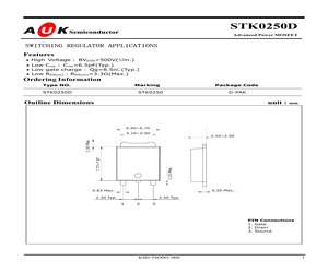
STK0250D Semiconductor Advanced Power MOSFET SWITCHING REGULATOR APPLICATIONS Features * * * * High Voltage : BVDSS=500V(Min.) Low Crss : Crss=6.5pF(Typ.) Low gate charge : Qg=8.5nC(Typ.) Low RDS(on) : RDS(on)=3.3(Max.) Ordering Information Type NO. Marking STK0250D Package Code STK0250 D-PAK Outline Dimensions unit : mm 6.50~6.70 5.10~5.50 1.15 Max. 7.77~7.97 1.18 Max. 2.10~2.50 0.55 Max. 0.83 Max. 2.30 Typ. 2.30 Typ. 1 2 3 PIN Connections 1. Gate 2. Drain 3. Source KSD-T6O001-000 1 STK0250D Absolute maximum ratings (Tc=25C) Characteristic Symbol Rating Unit Drain-source voltage VDSS 500 V Gate-source voltage VGSS 30 V (Tc=25) 2.0 A (Tc=125) 1.7 A * IDP 8.0 A Drain Power dissipation PD 35 W Drain current (DC) ID Drain current (Pulsed) Avalanche current (Single) IAS 2.0 A Single pulsed avalanche energy EAS 59 mJ Avalanche current (Repetitive) IAR 2.0 A Repetitive avalanche energy EAR 3.0 mJ TJ Tstg 150 -55~150 C Junction temperature Storage temperature range * Limited by
 8 Pages, 453 KB, Original
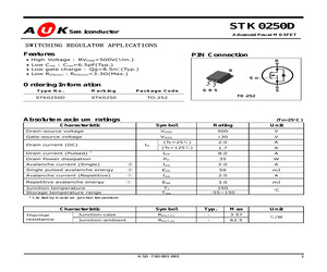
STK0250D Semiconductor Advanced Power MOSFET SWITCHING REGULATOR APPLICATIONS Features * * * * PIN Connection High Voltage : BVDSS=500V(Min.) Low Crss : Crss=6.5pF(Typ.) Low gate charge : Qg=8.5nC(Typ.) Low RDS(on) : RDS(on)=3.3(Max.) D D G Ordering Information Type No. Marking Package Code STK0250D STK0250 TO-252 GDS S TO-252 Absolute maximum ratings (Tc=25C) Characteristic Symbol Rating Unit Drain-source voltage VDSS 500 V Gate-source voltage VGSS 30 V (Tc=25) 2.0 A Drain current (DC) ID (Tc=125) 1.7 A * IDP 8.0 A Drain Power dissipation PD 35 W Drain current (Pulsed) Avalanche current (Single) IAS 2.0 A Single pulsed avalanche energy EAS 59 mJ Avalanche current (Repetitive) IAR 2.0 A Repetitive avalanche energy EAR 3.0 mJ TJ Tstg 150 -55~150 C Junction temperature Storage temperature range * Limited by maximum junction temperature Characteristic Thermal resistance Symbol Typ. Max Junction-case Rth(J-C) - 3.57 Junction-ambient Rth(J-a) - 62.5 KSD-T6O001-001 Unit /W 1 STK0250D
 8 Pages, 420 KB, Original


